Career Knowledge Partnership
Current Sensors · Open Loop · PCB Mount

KHTB / KHTC Series

Two compact PCB current-sensing architectures built around a common high-performance platform.

The KHTB and KHTC families are open-loop Hall-effect current transducers designed for precise electronic measurement of DC, AC, pulsed and mixed currents. Both families provide galvanic isolation between the primary high-power circuit and the secondary electronics, with a proportional analog output centred on a 2.5 V offset.

100–250 ANominal current range
Up to ±500 AMeasuring range
300 kHzTypical bandwidth
1 µsTypical response time
4.0 kVGalvanic isolation
5 VSingle supply
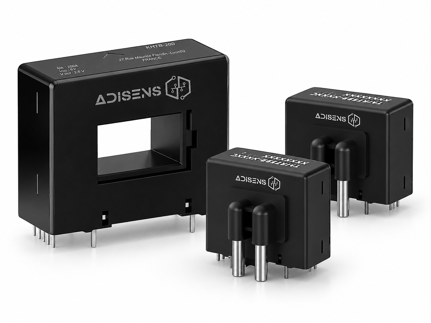
ADISENS KHTB and KHTC PCB current sensor families
Shared engineering platform

Fast, isolated current measurement for compact power electronics

KHTB and KHTC share the same core measurement philosophy: fast open-loop Hall-effect sensing, high linearity, galvanic isolation and a compact PCB-mount format.

±0.15% typ.Linearity performance
2.5 VOutput offset / reference level
16 mA typ.Current consumption
−40°C to +85°COperating temperature
Choose the right architecture

KHTB or KHTC?

The electrical performance is closely aligned, while the primary-current integration differs. Select the mechanical architecture that best fits your PCB and conductor arrangement.

Select a product family below to access reference-level specifications and datasheets.

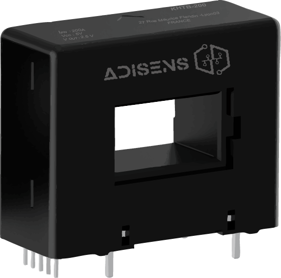
ADISENS KHTB current sensor
KHTB SERIES

Busbar / cable aperture architecture

KHTB uses a central aperture for the primary conductor. A busbar or primary cable passes through the sensor body, making the family suitable where the conductor is already part of the system architecture.

  • 100 A, 150 A, 200 A and 250 A nominal ratings
  • Measuring ranges up to ±500 A
  • 5 V supply and 2.5 V centred analog output
  • 300 kHz bandwidth and 1 µs typical response
  • 4 kV dielectric strength
Explore KHTB Series →
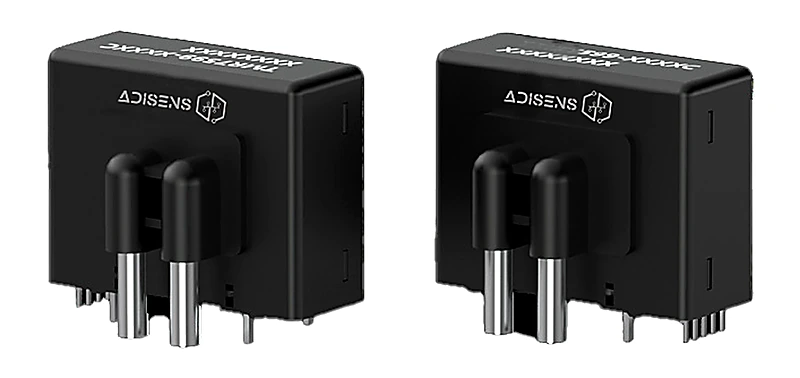
ADISENS KHTC current sensor
KHTC SERIES

Integrated primary-terminal architecture

KHTC integrates dedicated through-hole primary-current terminals into the PCB package. This architecture is intended for designs where the current path is routed directly through the sensor terminals on the board.

  • 100 A, 150 A, 200 A and 250 A nominal ratings
  • Measuring ranges up to ±500 A
  • 5 V supply and 2.5 V centred analog output
  • 300 kHz bandwidth and 1 µs typical response
  • 4 kV dielectric strength
Explore KHTC Series →
Application Focus · Solar Energy

Compact current sensing inside photovoltaic power-conversion systems

KHTB and KHTC are particularly relevant to solar-inverter architectures where isolated current feedback, compact PCB integration and fast response are required. The two mechanical approaches allow the designer to select either a pass-through primary conductor or an integrated primary-terminal arrangement.

Explore Solar Energy Applications →
KHTB and KHTC current sensors for solar inverter applications
Standards & compliance

Designed for integration into demanding electrical systems

The validated KHTB and KHTC technical documentation references IEC 61010-1 and EN 50178. CE conformity information and RoHS / REACH environmental declarations are available from ADISENS.

IEC 61010-1Electrical-safety reference
EN 50178Power-electronics equipment reference
CEConformity information available on request
RoHS / REACHEnvironmental declarations available on request
Continue to the product family

Select the mechanical configuration that matches your design